

Abstract
The piezoelectric response, conductivity and surface potential of individual grains and grain boundaries in free-standing polycrystalline ZnO nano- and microstructured platelets is studied using scanning probe based techniques on the nanoscale. We find that applied dc electric fields can alter the piezoresponse in individual grains, as well as the local nanoscale conductivity, and invert the relative surface potential at grain boundaries. This can be attributed to defect accumulation at the grain surfaces and at grain boundaries and the associated density of carriers. Together with recently observed below-bandgap photoconductivity at grain boundaries, the presented observation opens new venues for potential nanoelectronic applications that rely on grain and grain boundary engineering and functionality in a wide-bandgap transparent material.
Export citation and abstract BibTeX RIS
Introduction
Nano- and microstructures made from wide band gap (∼3.37 eV) zinc oxide (ZnO) exhibit many interesting properties suitable for electronics, optoelectronics; luminescent, biomedical and other applications [1]. Due to the material's non-centrosymmetric hexagonal-wurtzite crystal structure, ZnO nano- and microstructures exhibit piezoelectric properties which have received immense interest regarding piezotronic and energy harvesting applications [2]. ZnO has also shown ferromagnetic properties with and without doping of magnetic elements such as Mn, Ni, Co and Fe [3, 4] and it was reported that grain boundaries can cause ferromagnetic behaviour of ZnO [3]. Many types of complex shaped nano- and microstructures have already been synthesized and accordingly utilized for a wide range of applications [5]. Because of these excellent properties, ZnO nano- and microstructures in various forms have been widely used in numerous devices such as sensors, photo detectors [6, 7], gas sensors [8], and piezoelectric transducers [9], to name only a few. Harvesting mechanical energy with piezoelectric materials in nano- and micro-scale devices has seen significant interest in today's technologies [10–14]. These nano-micro devices are used e.g. for medical purposes to replace invalid human organs or even in wireless systems in which there is a need to be self- powered in order to remain active [15].
Among the variety of available piezoelectric materials, zinc oxide (ZnO) has many advantages for applications in electronic devices because of its growth versatility and huge abundance. The natural property of piezoelectricity of ZnO which is generating electrical current in face of mechanical stress made it a promising candidate in energy harvesting. ZnO is a nontoxic, biocompatible and biosafe semiconductor, and therefore can be used in biomedical applications [16, 17]. Moreover, ZnO can be found in many different configurations and structures, such as nanowires [18], nanobelts [19], nanorings [20], tetrapods [21] and nanohelices [22]. This makes ZnO a very suitable and flexible material to use in different applications.
Recently, in a detailed report, we showed interesting photoconductive properties of ZnO nano- and microstructured platelets by conductive atomic force microscopy (c-AFM) in dark and under laser illumination below the band gap [23]. In the present work we continue our study on ZnO platelet samples and look into their piezoelectric properties at the nanoscopic dimensions.
Experiment
ZnO nano-micro structural platelets were grown by flame transport synthesis (FTS). The details of the growing process can be found elsewhere [23, 24]. Piezoresponse force measurements (PFM) were performed by a commercial AFM system (AIST-NT Smart SPM 1000) under ambient conditions. Grounded platinum coated tips were used as a conductive probe in contact mode in order to image the piezoelectric response by PFM. An ac voltage was applied to excite surface oscillations of the material via the inverse piezoelectric effect. The amplitude and frequency of the applied ac voltage were 1–3 V and 100 kHz, respectively. The driving frequency was chosen to be very far from the contact resonance between tip and the sample in order to avoid possible artefacts of the PFM results. Both, the vertical PFM (VPFM) and lateral PFM (LPFM) were acquired on the ZnO nano- and microstructured platelets simultaneously.
The morphology of the grown ZnO nano- and microstructured platelets was investigated by scanning electron microscopy (SEM) using an Ultra Zeiss Plus SEM at 8 kV acceleration potential, and transmission electron microscopy (TEM) using a JEM-2200FS at 200 kV with omega-filter providing zero-loss peak high resolution imaging.
Results and discussion
The micro-scale morphology of the FTS grown ZnO nano- and microstructured platelets was investigated by SEM and results of typical samples are shown in figure 1. The platelet consists of structurally connected columnar grains as seen in top-view and angled view (high magnification) SEM images. The growth mechanism of these nano- and microstructured ZnO platelets and other structural evolutions have been discussed in a previous work [23].

Figure 1. (a) Top view SEM image, (b) angled view SEM showing the quasi-columnar structure of the ZnO sample ([21] John Wiley & Sons).
Download figure:
Standard image High-resolution imageThe microstructural evolution of the nano- and microstructured ZnO platelets was investigated in detailed using TEM. Figure 2 shows the results of the TEM results from the ZnO platelet, i.e., the nanoscale structure of the grain boundaries (figure 2(b)). From the selected area electron diffraction (SAED) pattern (figure 2(c)), it can be seen that there is a grain boundary with a 13.8° angle and coherent binding between the observed grains.

Figure 2. TEM image and SAED of a ZnO grain boundary. (a) Grain boundaries around several grains, (b) a single grain boundary, (c) selected local area diffraction (SAED) around a single grain boundary revealing the grain boundary angle.
Download figure:
Standard image High-resolution imageAfter morphological and microstructural characterizations, PFM were performed to gain the detailed insights into the nanoscale piezoresponse of these ZnO nano- and microstructured platelet samples within the single grains and around the grain boundaries. The out of plane and in plane component of the piezoresponse and associated polarization direction in the ZnO platelets can be easily separated by rotating the sample underneath the AFM cantilever in these measurements [25]. The VPFM detects vertical movement like deflection or buckling while the LPFM detects lateral movements like flexural buckling or lateral twisting. The effect of VPFM is independent of the cantilever scan direction. So the buckling contribution can be distinguished from twisting contribution by rotating the sample. Figure 3 shows the PFM results for the rotation of the ZnO nano- and microstructured platelet sample at different angles under the AFM cantilever for the same position of the sample surface.
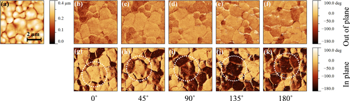
Figure 3. Angle-dependent PFM measurements. (a) Topography image, (b)–(k) PFM phase images for different rotation angels of the ZnO sample. The same grain during the rotation is shown by a white dotted circle.
Download figure:
Standard image High-resolution imageNote that colour contrast in VPFM images do not change much during the rotation of sample. On the contrary, by rotating the sample the colour contrast in LPFM images changes significantly. The colour contrast for the grains reverses upon 180° rotation of the sample, confirming that this is real in-plane piezoresponse, i.e. the sample is indeed piezoelectric. This also means that the spontaneous polarization is mostly oriented in-plane in the samples under investigation.
In order to understand the nanoscale piezoresponse in ZnO nano- and microstructured platelets better, we performed local electrical poling experiments using c-AFM tips. We find that the applied dc electric fields can alter the piezoresponse in individual grains. As seen in figure 4(c), the response is drastically reduced after the application of a positive bias of +9 V in a square-shaped area (white dotted line). Interestingly, the piezoresponse in the affected areas can be recovered to the original state after an equal and opposite bias has been applied to the same area (figure 4(d)). This behaviour has been observed in other oxide materials and can be attributed to defect accumulation at the grain surfaces and the associated density of carriers [26–31], which can lead to a shorting or screening of the applied PFM ac voltage, and thus a decreased piezoresponse.

Figure 4. Modification of piezoresponse by electrical poling. (a) Topography, (b) in-plane PFM phase before poling, (c) +9 V was applied in dashed box area, (d) −9 V was applied in inner dashed box area.
Download figure:
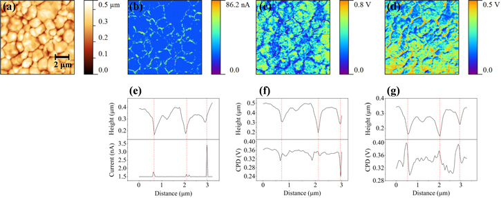
Standard image High-resolution imageIn order to study these effects further, we also performed Kelvin probe force microscopy measurements (KPFM) and corresponding obtained images are shown in figure 5. For simplicity of comparison, the cross section profiles are extracted on arbitrary grains for figures 5(b)–(d) and shown in figures 5(e)–(g), respectively. Each cross section profile comes with the cross section data of its topography image. The grain boundaries appear to have a lower contact potential difference (CPD) in KPFM images than the grain interiors in the as-grown state (figures 5(c) and (f)). After current has been passed through the conductive grain boundaries in figure 5(b), the subsequent KPFM images show a significant increase in CPD at the grain boundary (orange coloured boundaries in figure 5(d)) and an inverted relative potential contrast. By comparing the cross section profiles of figures 5(f) and (g), it is clear that at the grain boundaries the CPD has a significant change and it is increase after performing c-AFM, as seen by dips in the CPD in figure 5(f) turning to peaks in CPD in figure 5(g). Likely, this effect stems from deposited charge at the grain boundaries and field migration of defects along these [23, 32–34].
Figure 5. Modification of surface potential by electrical current. (a) Topography, (b) c-AFM image obtained with 1 V bias, (c) KPFM before c-AFM, (d) KPFM after c-AFM. Cross section data of (e) the current map, (f) KPFM image before c-AFM and (g) KPFM image after c-AFM.
Download figure:
Standard image High-resolution image
Conclusion
We report tuneable piezoelectric properties of individual grains and grain boundaries in self-supported polycrystalline ZnO nano- and microstructured platelets. It has been observed that that the applied dc electric fields can alter the piezoresponse of individual grains, as well as the local contact potential at the grain boundaries. This can be attributed to defect accumulation and the associated density of carriers. The fact that materials with piezoelectric response can be considered in using devices which generate electrical power from mechanical energy [35] makes these ZnO nano- and microstructured platelets very interesting for this purpose. The fact that this piezoelectric material is also transparent together with the recently observed below-bandgap photoconductivity at grain boundaries opens new venues for potential nanoelectronic applications that rely on grain and grain boundary engineering and functionality in a wide-bandgap transparent material.
Acknowledgments
We acknowledge support by the Australian Research Council through Discovery Grants. This work was also supported by the National Research Foundation of Korea funded by the Ministry of Education, Science, and Technology (contract no. NRF-2013S1A2A2035418). RA acknowledges the financial support from Deutsche Forschungsgemeinschaft (DFG), Germany in the CRC 1261 Project A5. We thank Hongwei Liu and Sean Lim (University of Sydney) for help with the TEM and SAED measurements.